
Click the icon to add a specified price to your Dashboard list. This makes it easy to keep track on the prices that matter most to you.

Toray Industries, Inc., announced that it is poised to begin mass-producing its STF-1000 photosensitive polyimide solution. This world-class offering is the fruit of the company’s ongoing drive to push the envelope with its proprietary negative-type photosensitive technology. It delivers patterning with an aspect ratio of 36 for films up to 500 micrometers thick. High-aspect-ratio patterning technology forms microstructures that are narrow and tall.
The company began shipping samples to customers last year for evaluations across electronic components, micro-electromechanical systems (MEMS) and diverse other applications. MEMS technology integrates micro-mechanical components, sensors, actuators, and other elements using microfabrication techniques developed for semiconductor devices.
Toray earned The Chemical Society of Japan Award for Young Chemists in Technical Development for 2025 for developing this high-aspect-ratio patterning technology while retaining the inherent advantages of a polyimide structure. These include excellent resistance to heat and chemicals, mechanical strength, insulation, and ultraviolet ray durability.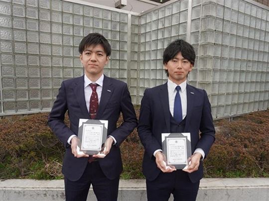
Photolithography produces high-resolution patterns over large areas in a single process by coating substrates with photosensitive materials, exposing them to light to form circuit patterns. This technique is common in manufacturing semiconductors, liquid crystal displays, and sensors.
In recent years, a rising need for microfabrication techniques to miniaturize and more densely integrate electronic components has driven the development of MEMS devices. This has fueled demand for photosensitive materials that can reliably withstand manufacturing processes and high-aspect-ratio patterning enabling microfabrication even for thick films. The issue with materials on the market has been that processing films with thicknesses exceeding 200 micrometers has often resulted in delamination from substrates or cracking.
This situation prompted Toray to enhance its polymer design technology for negative-tone formulation photosensitive materials. It created a photosensitive polyimide that can suppress pattern distortion and cracking even in thick films, culminating in an aspect ratio of 36 in films thicker than 200 micrometers. This material made it possible to form diverse patterns, including semiconductor vias and MEMS structures. The material also serves in scintillator panels in X-ray non-destructive testing equipment. Diverse prospective applications include advanced semiconductors and microfluidic devices. A scintillator panel is an X-ray imaging device component that emits visible light when X-rays strike it.
In 2025, Toray developed STF-2000, a photosensitive polyimide free of per- and polyfluoroalkyl substances, and has explored applications principally for electronic components and microfluidic devices.
Toray will leverage its core capabilities in synthetic organic chemistry, polymer chemistry, biotechnology, and nanotechnology in pursuing R&D into groundbreaking materials that can drive fundamental change in keeping with its enduring commitment to delivering new value and contributing to social progress.
Note: This story has not been edited by The Polymerupdate Editorial team and is auto-generated from a syndicated feed.